
Power device voltage derating for heavy-ion effects
Pick the technology class, the voltage rating, the LET your mission needs and the risk you accept. The tool returns the maximum operating voltage against single event burnout and gate rupture, from the Heavy-Ion Power Derating priors fitted to measured safe operating points, and compares the result with fixed derating rules.
This tool is provided as a free community resource. Results are population priors for a part you have not tested, not a substitute for testing your part. See Help & User Guide
Device
Mission requirement
Why the conventions behind this tool are what they are: the derating percentages, normal incidence for gate rupture, ion range, cold for burnout, latchup mistaken for burnout, lot traceability.
All technology classes at your LET and risk level
How it works
Estimating an operating voltage
Start from the technology class
Each class has its own fitted median and spread of the voltage fraction at which parts first fail, from interval censored test conditions, so parts that survived count as evidence.
Move it to your LET
The LET dependence is measured within parts tested at more than one LET, where part to part spread cannot hide it. The tolerable voltage generally falls as the LET rises, and is held flat above the top of the data.
Read off the risk you accept
The recommendation is the class's quantile at your risk times the rating, never above the rating, and flagged when it falls below the lowest voltage any part of the class was tested at.
Understanding the mechanisms
Understanding SEB and SEGR: an interactive model of the two failure modes this tool derates against
The advisor above fits measured safe operating points; the model below shows what those points are made of. In a vertical power MOSFET a heavy ion can turn on the parasitic transistor in the cell and start an avalanche that the drain supply feeds until the cell melts (single event burnout), or it can pile charge under the gate and, for picoseconds, add a share of the drain voltage to the field across the gate oxide (single event gate rupture). Silicon carbide devices burn out by a route that is still debated, at a voltage that barely depends on LET above about 10 MeV cm2/mg and that is a smaller share of the rating the higher the rating. Pick a mechanism, fire an ion, then move the sliders and watch which ones change the outcome.
Where a published expression exists (the gate rupture failure line, the ion-atomic-number oxide response, the silicon carbide burnout plateau and leakage onset) the model uses it; every other number is illustrative, chosen so that the direction and rough size of each effect follows the papers listed below, not to predict any device. It cannot tell you what a given part did, and its thresholds are not derating factors: those come from the fitted data above. The four beam presets use the LET against depth tables from the site's heavy-ion beam calculator; the free sliders use a smooth Bragg curve with the same shape. The silicon pane opens as a rotatable block cut at the strike (drag it, or switch to the flat section): its front face is the section, its top face the cell layout the ion sees, with an assumed 20 um stripe pitch that only the tilted track's lateral travel uses.
Where each effect in the model comes from
Burnout (silicon). The sequence of a track, holes crossing the body to its contact, a forward-biased source/body junction and electron injection is the analytical model of Hohl and Galloway [7]; the shift of the field peak to the epi/substrate interface under the injected current, and the regenerative avalanche there, is the current-induced avalanche that Wrobel and co-workers measured under dose rate [5] and the triggering analysis of Hohl and Johnson [8]; the first report and the drain-bias dependence are Waskiewicz and co-workers [6]. Kuboyama and co-workers measured the bias-dependent charge multiplication below the burnout voltage with EPICS [9]; they also found the transistor firing for any strike on the source from about a tenth of the rating and proposed a position-independent activation by the plasma column with a device constant threshold charge, a dissent from the body-resistance picture the model draws; their 2004 work [11] is on bipolar transistors and adds tunneling at the interface. The strike-position dependence in the model, with the neck and the channel edge most sensitive and the body-contact side least, follows the two-dimensional simulations of Roubaud, Dachs and co-workers [10] ("the most vulnerable areas are located in the neck and the channel regions") and the strike Luu and co-workers [13] chose next to the channel as among the most sensitive; the ratios are illustrative. The burnout voltage is the cell's second breakdown, independent of the ion once the LET exceeds about 20 (Liu, Titus and Boden [12]: the same 580 V for krypton and xenon from LET 20 to 63), and the n-buffer effect is theirs too; the model's floors, half of breakdown without a buffer and 0.85 with one, sit inside the measured range (about half for an IRF150 under Cf-252 [10], 0.6 of the rating for IRF150 and IRF450 parts [10], 0.72 and 0.85 of cell breakdown for 600 V prototypes without and with a buffer [12]). The wide spread of failure voltages across parts and ions, 22 to 90 percent of the measured breakdown in Fischer and co-workers [14] and 40 to 100 percent in Waskiewicz [6], summarized by Sexton [2], is the reason the advisor fits a distribution rather than a single threshold. Short-range ions under-test a part: bromine reaching the interface failed parts that Cf-252 fragments of the same LET did not [14], and the sensitive volume is the epi, about 80 percent of which must be crossed at rated bias [13]. The weak rise of the burnout voltage with temperature (burnout is generally a cold-case effect) is the trend Sexton [2] and Titus [1] summarize from Johnson and co-workers (IEEE Trans. Nucl. Sci., vol. 39, no. 6, 1992, not in the list below). Not modeled: the angle (planar parts are generally least sensitive off-normal, but the review [1] names a V-groove part whose sensitivity rose with angle, and no effective-LET law applies), the ion-species effect on burnout reported in [1], and the sustained, non-destructive current state between a pulse and burnout that [6], [8] and [10] describe and that a large load resistance favors.
Gate rupture (silicon). The two-part mechanism, an epitaxial response in which the drain bias is transiently coupled into the oxide by holes piling against the Si/SiO2 interface in the neck, combined with the ion's own weakening of the oxide, is the conceptual model of Brews and co-workers [16], evaluated in two dimensions by Allenspach and co-workers [17]; the coupling peaks within a few picoseconds and decays over tens to hundreds of picoseconds [16], [17], [21], and how long the field must persist to rupture the oxide is not known [16]. Fischer and co-workers found the effect in 1987 with 330 MeV gold [14]. The failure line the model draws is the published semi-empirical expression of Wheatley, Titus and Burton [18]: in the gate against drain plane the onset of rupture is a straight line whose slope, the coupled share of the drain bias, is 0.87 (1 - exp(-LET/18)) in the 1995 fit over five oxide thicknesses (0.84 and 17.8 in the 1994 fit on the 50 nm devices alone), and whose intercept at zero drain bias, the capacitor response, is 10 MV/cm times the oxide thickness divided by 1 + LET/53; the intercept scales with oxide thickness and the slope does not [18]. Titus and co-workers later wrote the capacitor response in ion atomic number, 10 MV/cm divided by 1 + Z/44 (IEEE Trans. Nucl. Sci., vol. 45, no. 6, 1998), fitted for ions from nickel to gold, which Lauenstein and co-workers verified on a second vendor's part [24], Kuboyama and co-workers found within a few percent of a measured value [25], and the 2013 review [1] calls an accepted modification, since ions of equal LET but different Z rupture the oxide at different fields [24]; the model offers both, and its neon and argon presets extrapolate the Z form below its fitted range. The 10 MV/cm and 53 hold for 30 to 150 nm oxides; thin oxides withstand more [20]. Angle enters as the oxide term divided by cos to the power 0.7 of the strike angle [18], so an angled strike is less severe and normal incidence is the worst case, as Mouret and co-workers [17] also found; for capacitors at zero drain bias Wrobel [15] and Selva [21] found a plain inverse cosine. Titus and co-workers measured no temperature dependence [18], Wrobel [15] found the same capacitor threshold from -100 to 150 C, and the review [1] reports a slight easing when hot; the model has no temperature term, which is conservative. The slope was measured on one test device, a 7 um epi stripe cell with a 4.6 um neck chosen by its authors for a strong gate rupture response, and the review [1] notes that the coupled share depends on neck width and process; the model therefore scales the published slope by a device coupling share (the "Titus 1994 test device" button sets it to one and reproduces the published lines; the default of 0.2 for the 300 V class device is illustrative). The LET in the slope is taken as the mean LET over the epi, so that an ion that just penetrates the epi, its Bragg peak near the epi/substrate interface, couples more than one of the same surface LET that stops early or carries its energy far into the substrate: the worst-case energy of Titus and co-workers [19] and the review [1], with the epi charge confirmed as the driver and the substrate charge as secondary by Liu and co-workers [23] and Lauenstein and co-workers [24]; at zero drain bias the oxide term alone remains, as Selva and co-workers found [21]. The intrinsic thin-oxide response is Sexton and co-workers [20], its origin in Wrobel [15] and its atomistic picture in Beck and co-workers [22]. The post-irradiation gate stress the model offers is standard test practice [19], [24]; the model marks an oxide suspect within 15 percent of its critical field, and fails the stress only for oxides under 30 nm, since the review [1] reports no loss of dielectric strength in thicker oxides irradiated below the critical voltage and Wrobel [15] found no sub-threshold damage in capacitors. A check on derating from Lauenstein and co-workers [24]: a 0.75 factor on the drain bias, applied to accelerator data, bounded the simulated on-orbit gold case for a hardened 200 V part with no margin to spare, and did not bound it for a commercial 500 V p-channel part. Not modeled: the alternative failure site over the body diffusion with hot-carrier injection proposed by Kuboyama and co-workers [25], who located the leakage path over the body edge rather than the neck and flag the mechanism as needing validation on n-channel parts; the review does not cite it and the two views are unreconciled.
Burnout (silicon carbide). The observable is a burnout voltage nearly independent of LET above about 10 MeV cm2/mg and the same for a MOSFET and a JBS diode of the same technology: about 500 V for a 1200 V MOSFET (Witulski and co-workers [29]), the same in the matching JBS diode with or without a drain resistor (Ball and co-workers [31]), and across five parts rated 1200 to 4500 V a plateau of 1.1e8 N^(-1/3) volts in the epi doping N, which the model uses as published (Kosier and co-workers [33]); as a share of breakdown that plateau falls with the rating, so higher-voltage SiC parts need more derating. Below LET 10 the threshold rises, to 600 and 900 V at LET 6.9 and 3.6 on a 1200 V MOSFET (Mizuta and co-workers [27]) and above the rating at LET 2 [31]. Permanent leakage damage starts lower, at a voltage that depends on the LET and not on the rating, epi or doping: about 180 V for LET below 29 and 130 to 140 V at LET 62, the unifying result of Johnson and co-workers [31] over 600 to 1700 V diodes with the data of Kuboyama and co-workers [26] and Javanainen and co-workers [28], whose peak-power scaling (bias squared times energy deposited per unit length) it rests on; the model uses the square root of 1e6 divided by LET, in volts. No burnout and no damage follow unless the ion crosses the whole epi [31], [33]; normal incidence is the worst case [31]. Because MOSFETs and diodes fail alike, Ball [31] argues that a parasitic transistor is not required, while Witulski [29] attributes the MOSFET case to parasitic transistor turn-on driving avalanche at the epi/substrate junction. The picture the model draws, the discharge of the energy stored in the depletion region through the track [33] as a localized energy pulse [31], with impact ionization clamping the field in SiC near 3 MV/cm against 0.3 MV/cm in silicon so that the power density is about a hundred times higher [30], [34], and a hot spot that passes the temperature at which SiC decomposes, is one of several proposed mechanisms; the hot spot sits under the Schottky contact in diodes [29], [30], [34], at the epi/substrate interface in an unbuffered MOSFET [29], [31], [32], and in the upper drift region when a buffer layer takes the field peak off the interface [32]. The model shows the observable and draws one proposal; the mechanism is not settled.
The reviews [1] to [4] cover both silicon mechanisms and the modeling behind them. Device physics used throughout: the one-sided abrupt-junction breakdown, critical field and depletion-width approximations for silicon are the textbook forms (Sze); for 4H-SiC the model scales the critical field with doping, 2.3 MV/cm at 1e16 cm-3, to reproduce the planar breakdown fit of Kosier and co-workers [33]; a real rating sits below the breakdown the model computes.
- J. L. Titus, "An Updated Perspective of Single Event Gate Rupture and Single Event Burnout in Power MOSFETs," IEEE Trans. Nucl. Sci. 60(3), p. 1912, 2013.
- F. W. Sexton, "Destructive Single-Event Effects in Semiconductor Devices and ICs," IEEE Trans. Nucl. Sci. 50(3), p. 603, 2003.
- G. H. Johnson, J. M. Palau, C. Dachs, K. F. Galloway, R. D. Schrimpf, "A Review of the Techniques Used for Modeling Single-Event Effects in Power MOSFETs," IEEE Trans. Nucl. Sci. 43(2), 1996.
- J. L. Titus, C. F. Wheatley, "Experimental Studies of Single-Event Gate Rupture and Burnout in Vertical Power MOSFETs," IEEE Trans. Nucl. Sci. 43(2), p. 533, 1996.
- T. F. Wrobel, F. N. Coppage, G. L. Hash, A. J. Smith, "Current Induced Avalanche in Epitaxial Structures," IEEE Trans. Nucl. Sci. 32(6), p. 3991, 1985.
- A. E. Waskiewicz, J. W. Groninger, V. H. Strahan, D. M. Long, "Burnout of Power MOS Transistors with Heavy Ions of Californium-252," IEEE Trans. Nucl. Sci. 33(6), p. 1710, 1986.
- J. H. Hohl, K. F. Galloway, "Analytical Model for Single Event Burnout of Power MOSFETs," IEEE Trans. Nucl. Sci. 34(6), p. 1275, 1987.
- J. H. Hohl, G. H. Johnson, "Features of the Triggering Mechanism for Single Event Burnout of Power MOSFETs," IEEE Trans. Nucl. Sci. 36(6), p. 2260, 1989.
- S. Kuboyama, S. Matsuda, T. Kanno, T. Ishii, "Mechanism for Single-Event Burnout of Power MOSFETs and Its Characterization Technique," IEEE Trans. Nucl. Sci. 39(6), p. 1698, 1992.
- F. Roubaud, C. Dachs, J.-M. Palau, J. Gasiot, P. Tastet, "Experimental and 2D Simulation Study of the Single-Event Burnout in N-Channel Power MOSFETs," IEEE Trans. Nucl. Sci. 40(6), p. 1952, 1993; C. Dachs et al., "Evidence of the Ion's Impact Position Effect on SEB in N-Channel Power MOSFETs," IEEE Trans. Nucl. Sci. 41(6), p. 2167, 1994.
- S. Kuboyama, N. Ikeda, T. Hirao, S. Matsuda, "Improved Model for Single-Event Burnout Mechanism," IEEE Trans. Nucl. Sci. 51(6), p. 3336, 2004.
- S. Liu, M. Boden, D. A. Girdhar, J. L. Titus, "Single-Event Burnout and Avalanche Characteristics of Power DMOSFETs," IEEE Trans. Nucl. Sci. 53(6), p. 3379, 2006; S. Liu, J. L. Titus, M. Boden, "Effect of Buffer Layer on Single-Event Burnout of Power DMOSFETs," IEEE Trans. Nucl. Sci. 54(6), p. 2554, 2007.
- A. Luu, P. Austin, F. Miller, N. Buard, T. Carrière, et al., "Sensitive Volume and Triggering Criteria of SEB in Classic Planar VDMOS," IEEE Trans. Nucl. Sci. 57(4), p. 1900, 2010.
- T. A. Fischer, "Heavy-Ion-Induced, Gate-Rupture in Power MOSFETs," IEEE Trans. Nucl. Sci. 34(6), p. 1786, 1987.
- T. F. Wrobel, "On Heavy Ion Induced Hard-Errors in Dielectric Structures," IEEE Trans. Nucl. Sci. 34(6), p. 1262, 1987.
- J. R. Brews, M. Allenspach, R. D. Schrimpf, K. F. Galloway, J. L. Titus, C. F. Wheatley, "A Conceptual Model of Single-Event Gate-Rupture in Power MOSFETs," IEEE Trans. Nucl. Sci. 40(6), p. 1959, 1993.
- M. Allenspach, J. R. Brews, I. Mouret, R. D. Schrimpf, K. F. Galloway, "Evaluation of SEGR Threshold in Power MOSFETs," IEEE Trans. Nucl. Sci. 41(6), p. 2160, 1994; I. Mouret et al., "Temperature and Angular Dependence of Substrate Response in SEGR," IEEE Trans. Nucl. Sci. 41(6), p. 2210, 1994.
- C. F. Wheatley, J. L. Titus, D. I. Burton, "Single-Event Gate Rupture in Vertical Power MOSFETs; An Original Empirical Expression," IEEE Trans. Nucl. Sci. 41(6), p. 2152, 1994; J. L. Titus, C. F. Wheatley, D. I. Burton, I. Mouret, M. Allenspach, J. Brews, R. Schrimpf, K. Galloway, R. L. Pease, "Impact of Oxide Thickness on SEGR Failure in Vertical Power MOSFETs; Development of a Semi-Empirical Expression," IEEE Trans. Nucl. Sci. 42(6), p. 1928, 1995. The ion-atomic-number form of the capacitor response is J. L. Titus, C. F. Wheatley, K. M. Van Tyne, J. F. Krieg, D. I. Burton, A. B. Campbell, "Effect of Ion Energy upon Dielectric Breakdown of the Capacitor Response in Vertical Power MOSFETs," IEEE Trans. Nucl. Sci. 45(6), p. 2492, 1998, as given in [1].
- J. L. Titus, C. F. Wheatley, M. Allenspach, et al., "Influence of Ion Beam Energy on SEGR Failure Thresholds of Vertical Power MOSFETs," IEEE Trans. Nucl. Sci. 43(6), p. 2938, 1996.
- F. W. Sexton, D. M. Fleetwood, M. R. Shaneyfelt, P. E. Dodd, G. L. Hash, "Single Event Gate Rupture in Thin Gate Oxides," IEEE Trans. Nucl. Sci. 44(6), p. 2345, 1997.
- L. E. Selva, G. M. Swift, W. A. Taylor, L. D. Edmonds, "On the Role of Energy Deposition in Triggering SEGR in Power MOSFETs," IEEE Trans. Nucl. Sci. 46(6), p. 1403, 1999.
- M. J. Beck, B. R. Tuttle, R. D. Schrimpf, D. M. Fleetwood, S. T. Pantelides, "Atomic Displacement Effects in Single-Event Gate Rupture," IEEE Trans. Nucl. Sci. 55(6), p. 3025, 2008.
- S. Liu, J. L. Titus, M. Zafrani, H. Cao, D. Carrier, P. Sherman, "Worst-Case Test Conditions of SEGR for Power DMOSFETs," IEEE Trans. Nucl. Sci. 57(1), p. 279, 2010.
- J.-M. Lauenstein, R. L. Ladbury, N. Goldsman, et al., "Interpreting Space-Mission LET Requirements for SEGR in Power MOSFETs," IEEE Trans. Nucl. Sci. 57(6), p. 3443, 2010; J.-M. Lauenstein, N. Goldsman, S. Liu, et al., "Effects of Ion Atomic Number on Single-Event Gate Rupture (SEGR) Susceptibility of Power MOSFETs," IEEE Trans. Nucl. Sci. 58(6), p. 2628, 2011.
- S. Kuboyama, N. Ikeda, E. Mizuta, H. Abe, T. Hirao, T. Tamura, "Rediscovery of Single-Event Gate Rupture Mechanism in Power MOSFETs," IEEE Trans. Nucl. Sci. 59(4), p. 749, 2012.
- S. Kuboyama, C. Kamezawa, N. Ikeda, T. Hirao, H. Ohyama, "Anomalous Charge Collection in Silicon Carbide Schottky Barrier Diodes and Resulting Permanent Damage and Single-Event Burnout," IEEE Trans. Nucl. Sci. 53(6), p. 3343, 2006.
- E. Mizuta, S. Kuboyama, H. Abe, Y. Iwata, T. Tamura, "Investigation of Single-Event Damages on Silicon Carbide (SiC) Power MOSFETs," IEEE Trans. Nucl. Sci. 61(4), p. 1924, 2014.
- A. Javanainen, K. F. Galloway, C. Nicklaw, et al., "Heavy Ion Induced Degradation in SiC Schottky Diodes: Bias and Energy Deposition Dependence," IEEE Trans. Nucl. Sci. 64(1), p. 415, 2017.
- A. F. Witulski et al., "Single-Event Burnout of SiC Junction Barrier Schottky Diode High-Voltage Power Devices," IEEE Trans. Nucl. Sci. 65(1), p. 256, 2018; A. F. Witulski, D. R. Ball, K. F. Galloway, A. Javanainen, J.-M. Lauenstein, A. L. Sternberg, R. D. Schrimpf, "Single-Event Burnout Mechanisms in SiC Power MOSFETs," IEEE Trans. Nucl. Sci. 65(8), p. 1951, 2018.
- S. Kuboyama, E. Mizuta, Y. Nakada, H. Shindou, A. Michez, J. Boch, F. Saigné, A. Touboul, "Thermal Runaway in SiC Schottky Barrier Diodes Caused by Heavy Ions," IEEE Trans. Nucl. Sci. 66(7), p. 1688, 2019.
- D. R. Ball et al., "Ion-Induced Energy Pulse Mechanism for Single-Event Burnout in High-Voltage SiC Power MOSFETs and Junction Barrier Schottky Diodes," IEEE Trans. Nucl. Sci. 67(1), p. 22, 2020; R. A. Johnson et al., "Unifying Concepts for Ion-Induced Leakage Current Degradation in Silicon Carbide Schottky Power Diodes," IEEE Trans. Nucl. Sci. 67(1), p. 135, 2020.
- J. A. McPherson, C. W. Hitchcock, T. P. Chow, W. Ji, et al., "Ion-Induced Mesoplasma Formation and Thermal Destruction in 4H-SiC Power MOSFET Devices," IEEE Trans. Nucl. Sci. 68(5), p. 651, 2021.
- S. L. Kosier, A. Sengupta, D. R. Ball, et al., "Physical Model for SiC Power Device Heavy-Ion Burnout Based on Pre-Strike Depletion Capacitance Energy Storage," IEEE Trans. Nucl. Sci. 72(4), p. 1418, 2025.
- C. M. Marques, A. Michez, F. Wrobel, S. Kuboyama, et al., "Physical Explanation for the Higher Sensitivity to Ion-Induced Burnout in SiC Schottky Diodes Compared to Si Schottky Diodes," IEEE Trans. Nucl. Sci. 72(8), p. 2411, 2025.
What the recommendation is based on
How far below its voltage rating a power MOSFET, GaN or SiC transistor, or a rectifier should be operated so that heavy ions do not burn it out or rupture its gate. The recommendation comes from the Heavy-Ion Power Derating priors (HIPD 2026-09): an interval-censored fit to 1,819 safe-operating points from 1,161 device records (published papers and reports, and proprietary test reports), split into 13 technology classes, with the LET dependence measured within parts rather than across them. A vendor screen of 856 more points, all at one LET, is fitted as a separate variant that the Add vendor screen switch brings in. The methodology section documents every step.
How the numbers are computed the HIPD methodology, figures and tables
Methodology: the Heavy-Ion Power Derating priors (HIPD)
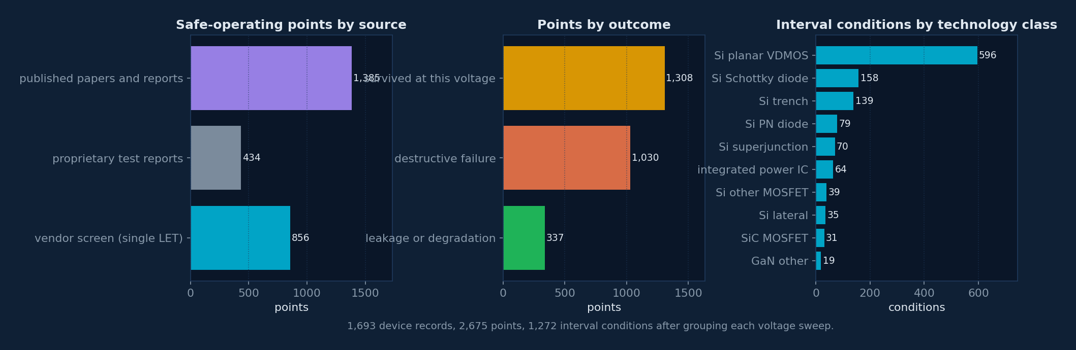
This page recommends how far below its voltage rating a power device should be operated so that a heavy ion does not destroy it. The recommendation comes from one machine-readable model file, hipd-2026-09.js (release 2026-09), which carries the fitted coefficients and the API the page calls. The model is an interval-censored fit to the 1,819 safe-operating points of 1,161 device records from published papers and reports and from proprietary test reports, grouped into 1,272 test conditions and split into 13 technology classes. A third-party vendor screen (856 points from 532 records, all at a single LET) is fitted alongside as a variant (1,672 conditions with it), which the tool uses only when its Add vendor screen switch is on; with it the corpus holds 2,675 points from 1,693 records. Two things distinguish the model from a flat derating rule: every test condition is treated as an interval rather than a value, so parts that survived count as evidence; and the dependence on LET is measured within parts rather than across them. Published sources are cited. Proprietary test reports and the vendor screen are identified only as such.
1. What the model answers
Two destructive heavy-ion mechanisms end the life of a power device. In single-event burnout a single ion turns on the parasitic bipolar transistor inherent in the vertical structure of a power MOSFET or the parasitic path in a rectifier, and the device sustains its own destructive current. In single-event gate rupture the ion track lets the gate dielectric see a field it cannot hold, and the oxide fails. Both depend strongly on the applied drain or reverse voltage, which is why the standard mitigation is not a hardened part but a derating: run the device far enough below its rating that the ion cannot start the process.
The question a designer asks is therefore "how far below". The usual answers are flat rules, most often 50 percent or 75 percent of the rating, applied without regard to technology or to the LET the mission requires. This model replaces the flat rule with a per-class distribution: for a stated technology class, LET requirement and accepted risk, the fraction of the rating at which that risk is met. It is a population prior for a part you have not tested. A part with its own heavy-ion qualification data should be used on that data.
2. Corpus and extraction
Every heavy-ion burnout and gate-rupture record on a power device was pulled from the combined test corpus that also underlies the SEL work: IEEE REDW and RADECS data-workshop papers, RADECS Proceedings and IEEE TNS papers, NASA Goddard radiation test reports, and proprietary test reports. A third-party vendor screen of commodity silicon MOSFETs, carried out entirely at a single LET, was added as a separate and clearly flagged source. Records were converted to structured safe-operating points under a written specification with explicit guard rules: never invent a number, never move a number between fields to complete a point, never treat a datasheet rating as a test voltage, and produce no point at all when the record states an outcome without the voltage at which it occurred. Roughly a quarter of records yielded no point for exactly that reason, most often because the source reports its voltage steps only in a figure.
3. Response and censoring
The modeled quantity is the fraction of the rating at which a part first shows an adverse response,
where Vadverse is the drain-source voltage, or the reverse voltage for a rectifier, and Vrated is the manufacturer maximum. Working in the fraction rather than in volts is what lets a 20 V trench MOSFET and a 1200 V silicon carbide MOSFET inform the same model.
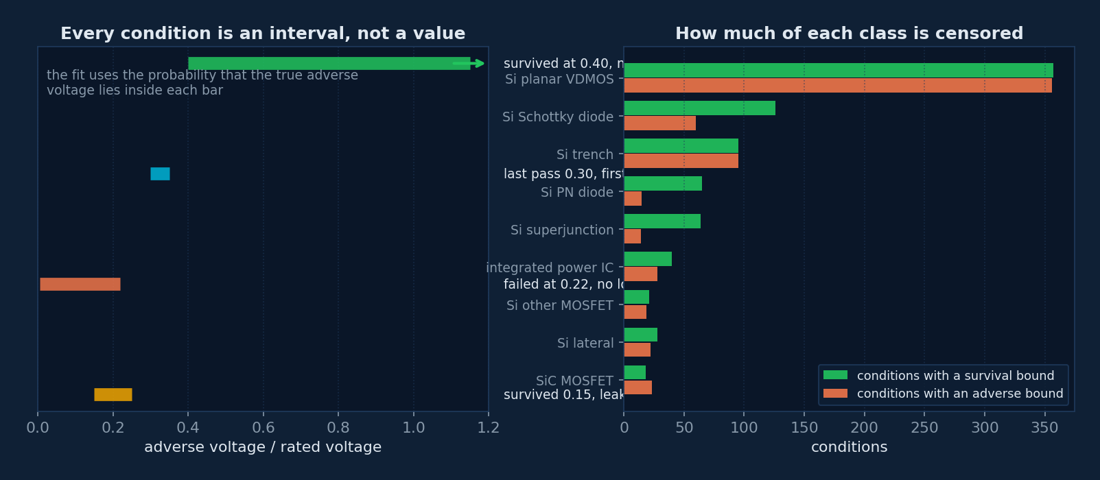
Almost no test reports the adverse voltage exactly. What a test reports is a sweep: the part survived at some voltages and failed at another, or it survived everything, or it failed at the first step tried. Each condition is therefore an interval:
failed at V: Vadverse ≤ V (left censored)
last pass V1, first fail V2: V1 < Vadverse ≤ V2
Points are grouped per record, LET and gate bias so that the two halves of one sweep become one interval rather than two independent observations, and the likelihood is the probability that the true adverse voltage falls inside each interval. Fitting only the observed failure voltages, which is what a naive average of published thresholds does, would bias the model low, because every part that survived its whole sweep would silently drop out.
4. The LET question
Parts are tested at whatever LET the facility and the program allowed. Some appear at a single LET, some at three or four, and the corpus spans LET 0.2 to about 110. Combining them requires a model of how the adverse voltage depends on LET, and the obvious approach fails.
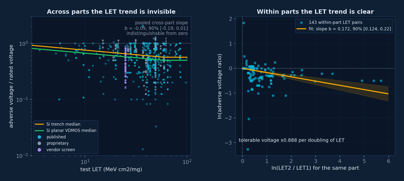
Across parts the LET trend is invisible. Pooling every condition and regressing on ln(LET) gives a slope of -0.09 with a 90 percent interval of [-0.19, 0.01], indistinguishable from zero, and a deviance against zero slope of 0.8. That is not because LET does not matter. It is because LET varies mostly between parts rather than within them, and the part-to-part spread is several times the LET effect. A robust part that happened to be tested only at high LET looks, to the pooled regression, like evidence that high LET is harmless.
Within parts the LET trend is clear. Restricting to parts tested at more than one LET at the same gate bias and taking the ratio of their adverse voltages differences out the part-to-part term. That gives
90 percent interval 0.114 to 0.212, from 135 within-part LET pairs
tolerable voltage multiplies by 0.893 per doubling of LET
Per class, where there are at least eight pairs: Si trench 0.169, Si planar VDMOS 0.141, integrated power IC 0.023. The wide-bandgap figure is worth watching but is not yet supported by enough pairs to publish as a separate slope, so a single global slope is used.
The mean model is therefore referenced to LET 37, the usual heavy-ion screening requirement:
y ~ Normal(mu, sclass)
so aclass is the log median adverse fraction at LET 37 and the reference point is the number designers already work to. Predictions are held flat above LET 60: published threshold-versus-LET curves saturate once an ion deposits more charge than the parasitic structure needs to trigger, and the corpus has too little data above 60 to fit the knee, so holding flat is the conservative reading. A saturating exponential form was tried first; its saturation length was not identified by this data and ran to infinity, which is why the reference form is used instead.
5. Technology classes
Enhancement-mode GaN is split into space-grade and commercial families, because the two behave as separate populations rather than as one spread: space-qualified parts survive their full rating to LET 85, while commercial parts fail between roughly 0.4 and 0.9 of rating. Fitting them together drove the scatter to the model bound and produced a tail quantile describing neither. Beyond that, structure matters more than material alone, so silicon MOSFETs are split by gate structure rather than lumped, gallium nitride is split by whether the part is a plain enhancement-mode HEMT or a cascode with a series silicon FET, and rectifiers are kept separate from transistors and split by material. Class intercepts are partially pooled toward the global mean by DerSimonian and Laird shrinkage (between-class spread tau = 0.4847), so thin classes are pulled toward the population rather than overfitted, and classes with fewer than ten conditions get no fit at all. Scatter is fitted per class where there are at least 25 conditions and is bounded; a class whose fitted scatter sits at the bound is flagged in the tool, because the data do not resolve it.
6. Time, and why there is no era term
The companion latchup model splits its populations at 2010, because latchup susceptibility turned out to depend on process generation. The same question was asked here three ways, and the answer is that this model carries no time term. The corpus is not short of history: 33 records from the 1990s, 294 from the 2000s, 677 from the 2010s and 157 from the 2020s.
A binary split is significant at every cut year, and the sign flips. Fitting a shared old-versus-new offset across the classes that have both sides gives, at a cut of 2005, newer parts tolerating 0.64 times the voltage; at 2010, 1.48 times; at 2015, 1.47; at 2018, 1.43. Every one of those is nominally significant by a likelihood-ratio test. A coefficient that changes sign depending on where the line is drawn is not measuring a trend in the devices.
Modeled continuously, the trend disappears. Replacing the binary split with publication year as a continuous covariate, over the six classes with at least 25 conditions and a decade of span, gives a trend of -0.12 per decade with a likelihood-ratio deviance of 3.8, which is not significant. If anything the point estimate leans very slightly the wrong way, toward newer parts tolerating less.
Where a per-class comparison is possible, the medians do not move; only the scatter does. Three classes have enough conditions on both sides of 2010. Silicon lateral: median 0.525 before against 0.526 after, which is no change at all, while sln falls from 0.56 to 0.20. Silicon planar VDMOS: median 0.561 against 0.498, very slightly worse, while sln falls from 1.57 to 1.18. Integrated power ICs go the other way on both counts, median 0.83 against 1.25 but sln rising from 0.66 to 1.67, so their tenth percentile actually drops by a factor 0.41. The apparent modern advantage in the binary fits was never a shift in central tendency. It was the older populations being more heterogeneous, which moves a tail quantile without moving the device physics.
Era is also largely aliased with technology. Silicon carbide MOSFETs, silicon carbide Schottky rectifiers, enhancement-mode GaN and silicon Schottky rectifiers have essentially no pre-2010 records in this corpus, and silicon trench has five. Those parts were not being heavy-ion tested for destructive effects before 2010 because, in flight-relevant form, they largely did not exist. A time term would therefore mostly re-encode the technology class the model already conditions on.
The practical consequence is that a designer should condition on technology, not on decade. Choosing a modern trench MOSFET over a 1990s planar one does not buy derating headroom; it changes which class applies, and the class numbers already say what that costs.
One caveat runs the other way and is not captured by any of the above. Within the wide-bandgap classes the technology genuinely did move fast, and the corpus is thin enough that a single early paper can dominate a class. The commercial GaN results here span 2016 to 2021 on roughly a dozen part types, and the earliest of them are devices that do not represent what is being bought today. At this sample size the model cannot separate that from ordinary part-to-part spread, so the GaN classes are flagged in the tool as thin and fast-moving, and they are the classes where part-specific test data should most strongly outrank the prior.
7. Results by class
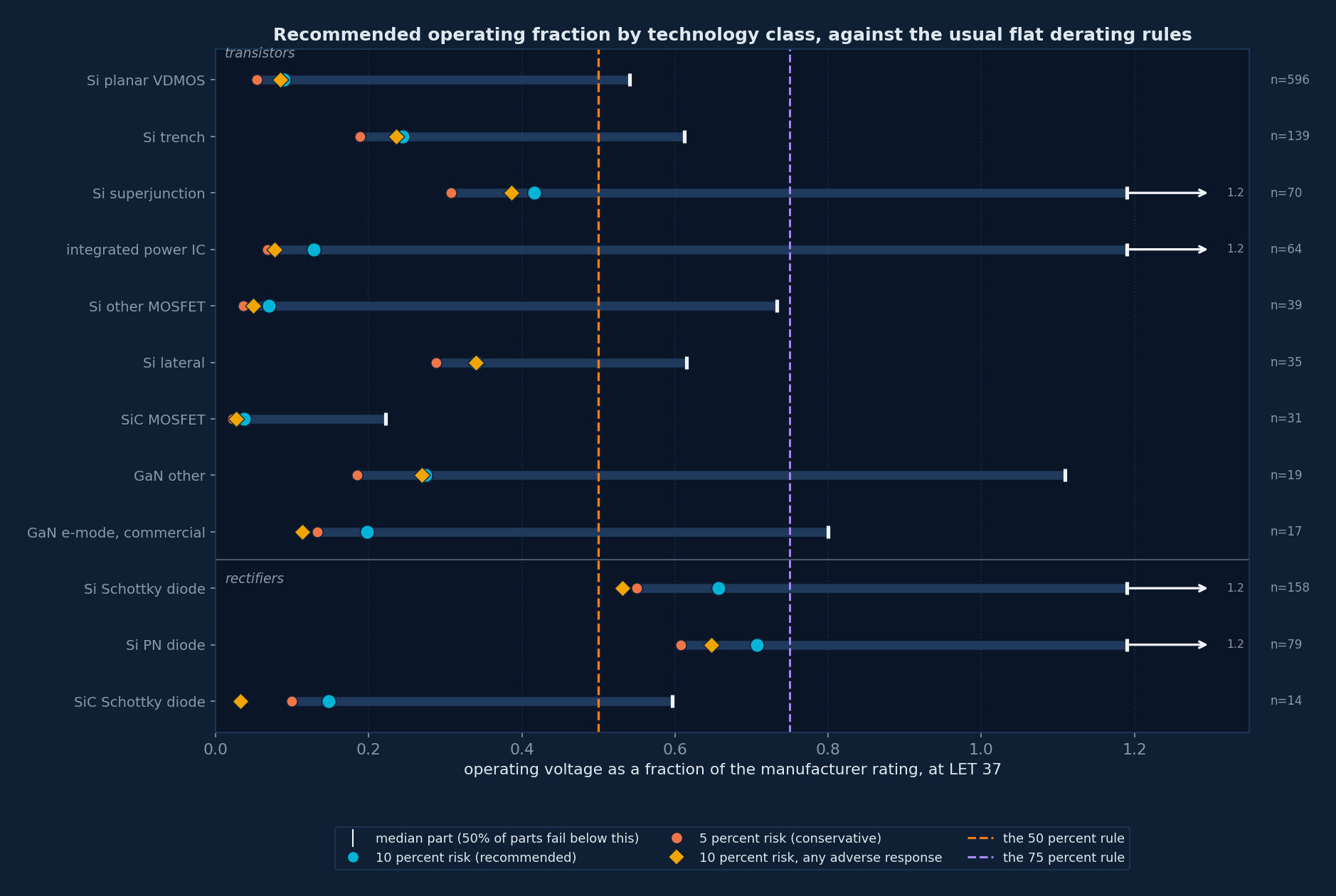
Table 1 gives the fitted numbers at the reference LET. The median column is the part in the middle of the class: half of the class is predicted to fail below it, so it is not a design point. The 10 and 5 percent columns are the design numbers, the fraction of the rating at which the modeled probability of an adverse response is held at or below that value. Where the median exceeds 1.0 the class as a whole tolerates its full rating at this LET and the derating question is answered by the electrical rating rather than by radiation.
Table 1. Fitted derating at LET 37, published and proprietary corpus (the default)
| Technology class | conditions | with an adverse outcome | tested LET range | median fraction | 10 percent risk | 5 percent risk | 10 percent, any adverse | sln |
|---|---|---|---|---|---|---|---|---|
| FAM | Silicon transistors | |||||||
| Si trench | 139 | 95 | 2.7 to 86 | 0.61 | 0.244 | 0.188 | 0.236 | 0.72 |
| Si planar VDMOS | 596 | 356 | 0.2 to 100 | 0.54 | 0.089 | 0.054 | 0.084 | 1.40 |
| Si superjunction | 70 | 14 | 21.3 to 98 | 1.20 | 0.416 | 0.308 | 0.386 | 0.83 |
| Si lateral | 35 | 22 | 5.7 to 44 | 0.61 | 0.340 | 0.288 | 0.340 | 0.46 |
| Si other MOSFET | 39 | 19 | 8.8 to 85.8 | 0.73 | 0.070 | 0.036 | 0.049 | 1.83 |
| FAM | Wide bandgap | |||||||
| SiC MOSFET | 31 | 23 | 3.6 to 65 | 0.22 | 0.037 | 0.023 | 0.027 | 1.39 |
| GaN other | 19 | 2 | 1.8 to 87 | 1.11 | 0.274 | 0.185 | 0.270 | 1.09 |
| FAM | Rectifiers | |||||||
| Si Schottky diode | 158 | 60 | 2 to 79 | 1.23 | 0.656 | 0.550 | 0.531 | 0.49 |
| Si PN diode | 79 | 15 | 15 to 84.4 | 1.21 | 0.707 | 0.607 | 0.648 | 0.42 |
| SiC Schottky diode | 14 | 6 | 2.8 to 57 | 0.60 | 0.148 | 0.099 | 0.033 | 1.09 |
| FAM | Integrated | |||||||
| integrated power IC | 64 | 28 | 19 to 110 | 1.20 | 0.128 | 0.068 | 0.077 | 1.74 |
Every recommendation is also checked against the observation floor, the lowest voltage fraction at which any part of that class was actually tested. A quantile below that floor is an extrapolation into a region the data do not cover, and the tool flags it rather than presenting it as an observation.
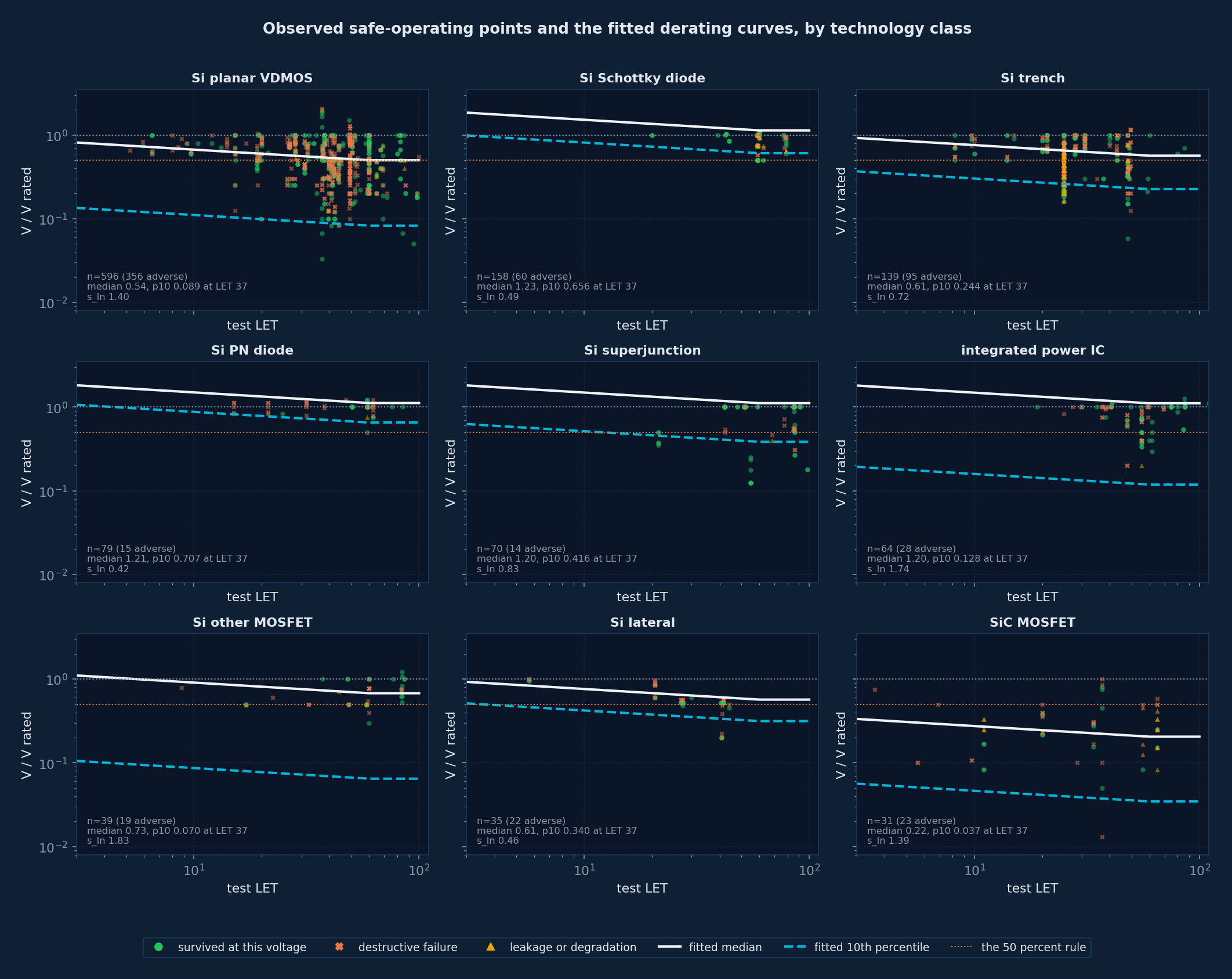
Table 2. How the 10 percent recommendation moves with the LET requirement
| Technology class | LET 10 | LET 20 | LET 37 | LET 60 and above |
|---|---|---|---|---|
| FAM | Silicon transistors | |||
| Si trench | 0.302 | 0.270 | 0.244 | 0.226 |
| Si planar VDMOS | 0.111 | 0.099 | 0.089 | 0.083 |
| Si superjunction | 0.514 | 0.460 | 0.416 | 0.384 |
| Si lateral | 0.421 | 0.376 | 0.340 | 0.315 |
| Si other MOSFET | 0.086 | 0.077 | 0.070 | 0.065 |
| FAM | Wide bandgap | |||
| SiC MOSFET | 0.046 | 0.041 | 0.037 | 0.035 |
| GaN other | 0.340 | 0.303 | 0.274 | 0.254 |
| FAM | Rectifiers | |||
| Si Schottky diode | 0.812 | 0.725 | 0.656 | 0.607 |
| Si PN diode | 0.875 | 0.781 | 0.707 | 0.653 |
| SiC Schottky diode | 0.183 | 0.163 | 0.148 | 0.136 |
| FAM | Integrated | |||
| integrated power IC | 0.159 | 0.142 | 0.128 | 0.118 |
The LET dependence is real but modest compared with the class differences and with the within-class spread. Going from LET 10 to LET 60 costs about 25 percent of the tolerable voltage, whereas moving between technology classes moves it by factors of several.
8. Against the flat derating rules
Figure 5 puts the fitted recommendations next to the flat rules. The rules are not uniformly wrong, they are wrong in both directions at once. Section 7 gives the numbers this rests on. For commodity trench silicon MOSFETs and for silicon carbide the 50 percent rule is badly optimistic: the fitted median part is already adverse at or below half its rating, so a designer following the rule is operating a coin flip. For silicon rectifiers the same rule is unnecessarily harsh, costing voltage headroom the data do not require. A rule that does not know the technology cannot be right for both.
9. The vendor screen
One source is a third-party screen of 532 commodity silicon MOSFETs carried out entirely at a single LET, with a voltage sweep per part. It is by far the largest single contribution to the silicon trench class and its method has not been independently verified, so it is excluded from the default fit and offered as an option, with the tool reporting both answers whenever a class contains any of it.
Two features of that screen required care. First, more than half of its recorded failures are tagged as a protected, current-limited condition in which leakage or degradation was treated as the failure, rather than a confirmed destructive event. Second, and more consequentially, every sweep begins near 20 percent of the rating and 40 percent of its failures occur at that very first step. For those parts the adverse voltage is unresolved somewhere below the floor of the test, so the failure is not a measurement and it is excluded; retaining it would let the fitted lower tail be set by the floor of someone's test protocol rather than by the devices. Excluding the protected-condition rows instead, which sounds like the more obvious correction, makes matters worse: those rows carry the resolved higher-voltage failures, and what remains is dominated by the floor-pinned ones.
With the floor-pinned failures removed the two source variants agree far better than they did. For silicon trench at LET 37 and 10 percent risk the corpus alone gives 24% of rating and adding the screen gives 20%, against a factor of three disagreement before the correction.
Table 3. Sensitivity to the vendor screen, 10 percent recommendation at LET 37
| Technology class | conditions, corpus only | conditions with the screen added | of which vendor screen | corpus only | screen added | ratio |
|---|---|---|---|---|---|---|
| Si trench | 139 | 539 | 400 | 0.244 | 0.200 | x0.8 |
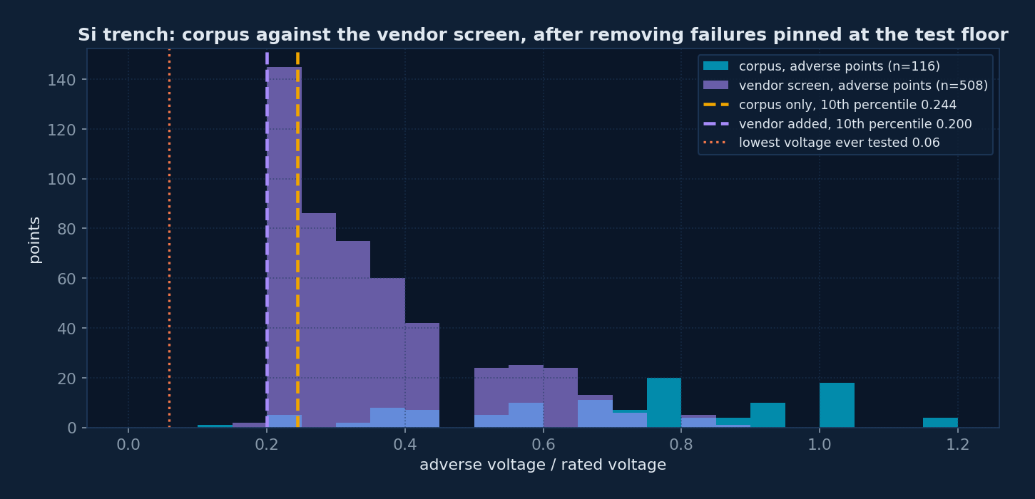
Neither answer is obviously the right one. A screen run to a fixed protocol on many parts will find failures that a published paper on a hand-picked part would not report, so some of the difference is genuine population selection rather than method. The conservative course is to take the lower of the two numbers unless there is a reason to prefer one source, and that is what the tool advises when the two disagree by more than about a factor of 1.5.
10. Burnout, gate rupture and leakage
The model is fitted twice. The catastrophic definition counts only burnout and gate rupture. The any adverse definition also counts a reported leakage or degradation onset, meaning a permanent parametric shift attributed to the ion but short of destruction. Which definition applies is a system question rather than a device question: a converter that can tolerate a few microamps of extra gate leakage for the rest of the mission should use the catastrophic definition, whereas a precision current path or a part whose leakage will run away with temperature should use the other.
The gap between the two is largest exactly where it should be. For silicon carbide MOSFETs the any-adverse recommendation is 1.4 times lower than the catastrophic one, because permanent gate and drain leakage increases in silicon carbide occur well below any destructive voltage and are widely reported. For silicon rectifiers the two definitions nearly coincide.
Mechanism screening carried over from the SEL work matters here in the opposite direction. Records where a voltage-swept destructive event in a smart-power or BCD part is burnout of an embedded DMOS device rather than latchup were adjudicated separately; the same signature that removes a part from the latchup statistics puts it into these. Post-irradiation gate-stress failures, where nothing happens in the beam but the part fails a subsequent stress, are recorded as degradation rather than as an in-beam failure unless the source itself calls them failures.
11. How the tool uses the model
The tool evaluates the fitted lognormal at your LET and risk level:
and multiplies by your voltage rating. Four guards apply. The recommendation is never allowed above the manufacturer rating, since the output is a maximum operating voltage and the electrical rating governs; when the risk quantile lands above the rating the tool says that no heavy-ion derating is indicated rather than inventing headroom. LET requests above 60 are held at 60 and flagged. A class whose fitted scatter sits at the model bound is flagged, because its tail quantile is then driven by the bound rather than by data. A recommendation below 5 percent of rating is flagged as effectively unusable, because at that point the honest engineering answer is a qualified part, a different technology, or protection that survives the event, not a derating.
The risk figure is the fraction of the tested part types in that class that were adverse at that voltage and LET, read as a probability for a part of the class whose own data are not in hand. It is a planning prior from a test archive, not a market sample: parts get tested because someone was concerned about them, and the archive is weighted accordingly. It is a per-part probability, not a mission rate. Converting to a mission rate needs the ion fluence the part will see, which is what the SEE Rate Assessment Tool does, and the number of such parts in the system, which is what the SEL Test-LET Tool does for latchup.
12. Limitations
Ion energy and range are not yet covariates. Burnout and gate rupture both depend on how deep the charge track runs, not only on surface LET. The corpus contains explicit counterexamples in which the same LET at different beam energies gave different threshold voltages. Energy, energy per nucleon and range in silicon are recorded per point where the source gave them, and will become covariates when the phase-two extraction fills them in for more records. Until then a recommendation based on low-energy beam data may be optimistic for the deep tracks of a real cosmic-ray environment.
Gate bias is recorded but not fitted. Gate rupture thresholds move strongly with the off-state gate voltage, and the corpus shows it clearly within individual sweeps. There are not yet enough conditions carrying both a gate bias and a bracketed threshold to fit it per class, so the model averages over the gate biases that were tested. A part run with a strongly negative gate bias sits at the pessimistic end of that average.
Angle and temperature are not covariates. Effective LET absorbs some of the angle effect where the source reported it that way. Temperature is recorded and is known to matter, but too few conditions carry it.
Class scatter is large and in several classes not resolved. The spread within a technology class is wider than the difference between classes for some pairs. That is a statement about commodity power devices rather than about the model: two parts with the same voltage rating from the same vendor in the same package can differ by an order of magnitude in burnout voltage. It is also why the recommendation sits in the lower tail rather than at the median.
Thin classes. SiC JFET, GaN cascode and IGBT have too few conditions to fit, and SiC Schottky and GaN classes rest on small samples whose intercepts are pulled substantially toward the population. Treat those numbers as indicative and weight any part-specific data heavily.
The voltage rating is the denominator, and it is not always verifiable. Every number here is a fraction of the manufacturer maximum rating, so the rating matters as much as the failure voltage. Where a source quotes a rating that has already been derated for space rather than the datasheet maximum, the fractions computed from it are biased and there is no way to tell from the record. For the corpus the ratings come from the part database and can be checked against datasheets. For the third-party vendor screen they cannot: only one of its 532 parts also appears in the corpus, so its ratings are unverifiable against any independent source. Their values do look like datasheet maxima rather than derated ones, since they include the odd but real figures a datasheet carries, but that is an impression rather than a check, and it is a further reason the screen is not the default.
This is a prior, not a qualification. It describes the historical population of tested power devices. It does not know about your lot, your bias conditions, your thermal design or your protection circuit, and it cannot substitute for testing a part you intend to fly.
13. Files and reproducibility
The site publishes one file for this model, hipd-2026-09.js. It carries the
fitted coefficients for both response definitions and both source variants, the DeratingModel API the
page calls, and the anonymized point cloud the charts draw, reduced to class, LET, voltage fraction, outcome and
source category. To check the tool against the model in a browser console,
DeratingModel(HIPD_MODEL).selftest() should report zero mismatches. No source data files are
published: a substantial part of the corpus is proprietary, the vendor screen belongs to a third party, and the
numbers quoted in this section are baked into the page at build time rather than served as a dataset.
14. References
[1] T. F. Wrobel, F. N. Coppage, G. L. Hash and A. J. Smith, "Current induced avalanche in epitaxial structures," IEEE Trans. Nucl. Sci., vol. 32, no. 6, 1985. The origin of single-event burnout in power devices.
[2] J. L. Titus and C. F. Wheatley, "Experimental studies of single-event gate rupture and burnout in vertical power MOSFETs," IEEE Trans. Nucl. Sci., vol. 43, no. 2, pp. 533-545, 1996. The response-surface description of gate rupture against drain and gate bias that the gate-bias caveat in Section 11 refers to.
[3] J. L. Titus, "An updated perspective of single event gate rupture and single event burnout in power MOSFETs," IEEE Trans. Nucl. Sci., vol. 60, no. 3, pp. 1912-1928, 2013. Review of mechanisms, test practice and the energy and range dependence.
[4] MIL-STD-750, Test Method 1080, Single-event burnout and single-event gate rupture testing of power MOSFETs. The stepped-voltage protocol that most of the corpus follows.
[5] JPL Publication 08-10, Single-event gate rupture test guideline, cited by several records in the corpus as the protocol used.
[6] NASA EEE-INST-002, Instructions for EEE parts selection, screening, qualification and derating, and ECSS-Q-ST-30-11C, Derating of electronic components. The sources of the flat derating rules compared in Section 7.
[7] IEEE Radiation Effects Data Workshop records and RADECS data-workshop records; RADECS Proceedings and IEEE Trans. Nucl. Sci.; NASA Goddard Space Flight Center radiation effects test reports. The published portion of the corpus, re-extracted from the primary documents.
[8] Proprietary heavy-ion test reports, and one third-party vendor heavy-ion screen carried out at a single LET. Used in aggregate only and never shown individually.
[9] R. DerSimonian and N. Laird, "Meta-analysis in clinical trials," Controlled Clinical Trials, vol. 7, no. 3, pp. 177-188, 1986. The shrinkage used for partial pooling of class intercepts.
[10] G. R. Allen, Heavy-Ion Power Derating priors (HIPD), release 2026-09, Space-RHA (this page and the model file).